Nope - I think confirmation of LWLG is more accurate...
I have no training in this field, but I think I see a connection here...
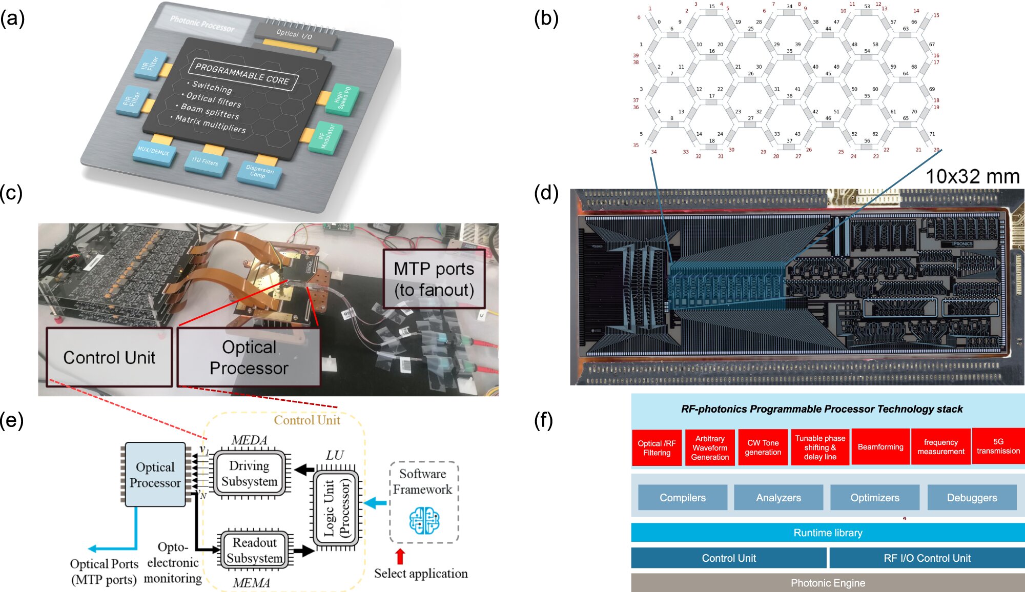
The photonic processor elements and layers. a Optical layer of the processor with the core, I/Os, and high-performance blocks, b schematic of the waveguide mesh core, c assembled chip with control unit and access fibers, d picture of the chip with the highlighted region of the reconfigurable core, e interconnection diagram between optical system, control unit and software layer, f Software layer stack employed in this work. Credit: Nature Communications (2024). DOI: 10.1038/s41467-024-45888-7
 News
News  Market Data
  Discover