


Wednesday, April 17, 2024 10:27:02 AM
I have no training in this field, but I think I see a connection here...
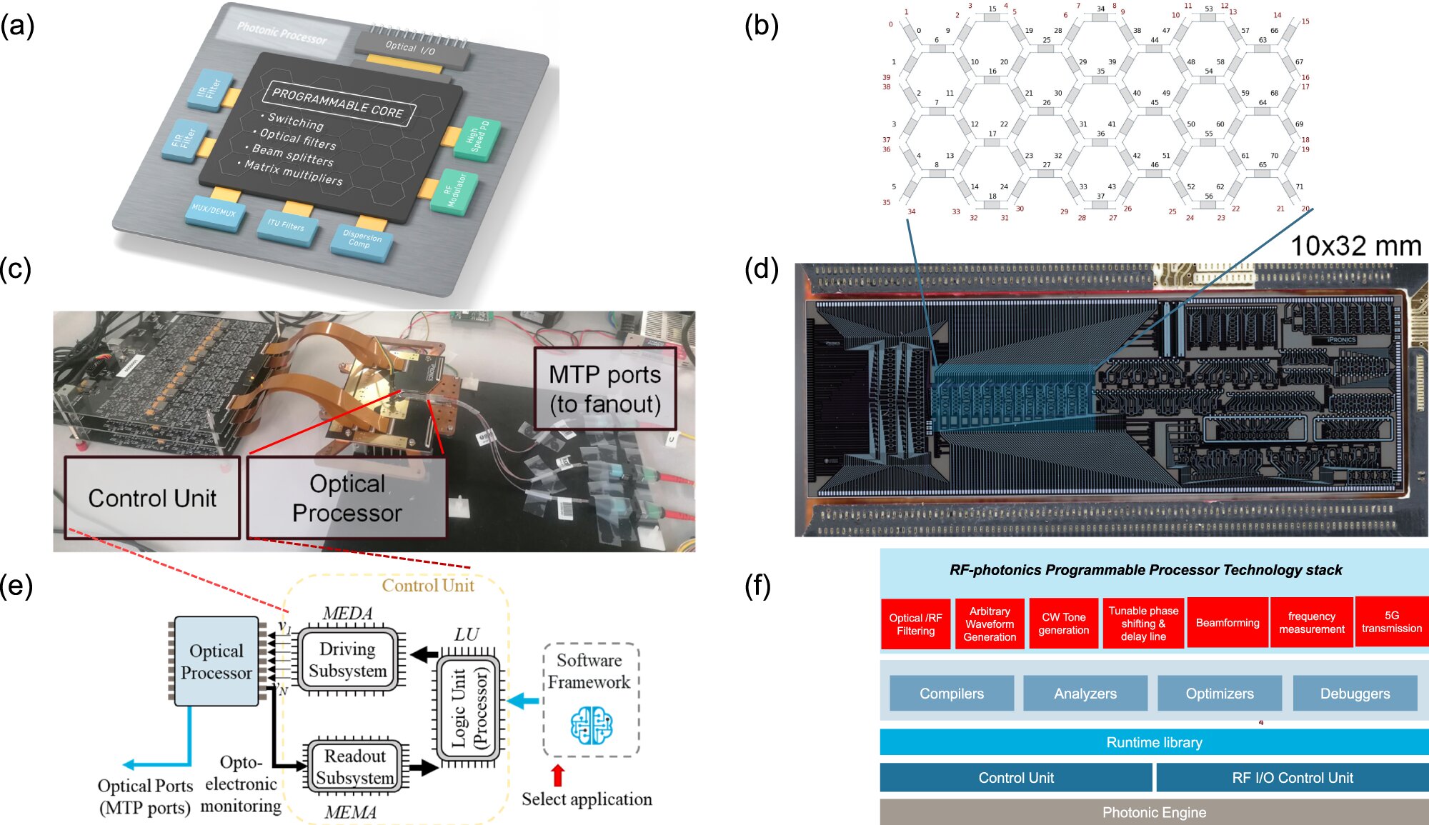
The photonic processor elements and layers. a Optical layer of the processor with the core, I/Os, and high-performance blocks, b schematic of the waveguide mesh core, c assembled chip with control unit and access fibers, d picture of the chip with the highlighted region of the reconfigurable core, e interconnection diagram between optical system, control unit and software layer, f Software layer stack employed in this work. Credit: Nature Communications (2024). DOI: 10.1038/s41467-024-45888-7
I would be happy to discuss this here: https://investorshub.advfn.com/Xenas-Study-Hall-29911

Recent LWLG News
- Lightwave Logic Reaffirms Commercialization Timeline Presented at the 2024 Annual Shareholder Meeting • PR Newswire (US) • 06/03/2024 12:31:00 PM
- Form 8-K - Current report • Edgar (US Regulatory) • 05/24/2024 08:01:14 PM
- Lightwave Logic and Advanced Micro Foundry (AMF) Partner to Accelerate Development of Silicon Photonics Modulators Using Electro-Optic Polymers • PR Newswire (US) • 05/21/2024 12:31:00 PM
- Lightwave Logic Provides First Quarter 2024 Corporate Update • PR Newswire (US) • 05/13/2024 12:31:00 PM
- Form 10-Q - Quarterly report [Sections 13 or 15(d)] • Edgar (US Regulatory) • 05/10/2024 08:41:09 PM
- Lightwave Logic Demonstrates Thought Leadership with Critical Contributions to Global Integrated Photonics Industry Roadmap • PR Newswire (US) • 04/16/2024 12:31:00 PM
- Lightwave Logic Secures New Patent for Diamondoid Non-linear Optical Chromophore Patent to Improves Material Robustness • PR Newswire (US) • 04/01/2024 12:31:00 PM
- Lightwave Logic EO Polymer Achieves World-Class Performance of 400Gbps with Plasmonic Mach Zehnder Modulator • PR Newswire (US) • 03/28/2024 12:31:00 PM
- Lightwave Logic Demonstrates World-Class 200Gbps Heterogeneous Polymer/Silicon Photonic Modulator Results • PR Newswire (US) • 03/25/2024 12:31:00 PM
- Lightwave Logic to Host Annual Meeting of Shareholders on May 22, 2024 • PR Newswire (US) • 03/19/2024 12:31:00 PM
- Lightwave Logic to Participate in Upcoming Investor Conferences • PR Newswire (US) • 03/15/2024 12:31:00 PM
- Lightwave Logic Provides Fourth Quarter and Fiscal Year 2023 Corporate Update • PR Newswire (US) • 03/01/2024 01:31:00 PM
- Form 10-K - Annual report [Section 13 and 15(d), not S-K Item 405] • Edgar (US Regulatory) • 02/29/2024 10:09:53 PM
- Form 4 - Statement of changes in beneficial ownership of securities • Edgar (US Regulatory) • 12/08/2023 09:00:04 PM
- Form 144 - Report of proposed sale of securities • Edgar (US Regulatory) • 12/07/2023 12:11:28 AM
- Lightwave Logic Issues Shareholder Letter and Provides Corporate Update • PR Newswire (US) • 12/04/2023 01:31:00 PM
- Small Cap Recipient of Military Drone Technology • InvestorsHub NewsWire • 11/20/2023 01:14:45 PM
- Epazz, Inc. (OTC Pink: EPAZ) ZenaDrone Demonstration to Defense Departments of UAE and Saudi Arabia • InvestorsHub NewsWire • 11/15/2023 12:19:31 PM
- Lightwave Logic Provides Third Quarter 2023 Corporate Update • PR Newswire (US) • 11/10/2023 01:31:00 PM
- Form 10-Q - Quarterly report [Sections 13 or 15(d)] • Edgar (US Regulatory) • 11/09/2023 09:24:23 PM
- Lightwave Logic to Participate in Upcoming Investor Conferences • PR Newswire (US) • 11/06/2023 01:31:00 PM
- Lightwave Logic CEO Dr. Michael Lebby to Present at the Optica Photonic-Enabled Cloud Computing Industry Summit • PR Newswire (US) • 10/12/2023 12:50:00 PM
- Lightwave Logic Receives 2023 Industry Innovation Award for Hybrid PIC/Optical Integration Platform at the European Conference on Optical Communications • PR Newswire (US) • 10/03/2023 12:31:00 PM
- Form 8-K - Current report • Edgar (US Regulatory) • 10/02/2023 08:00:08 PM
- Lightwave Logic to Participate in Upcoming Investor Conferences • PR Newswire (US) • 09/05/2023 12:31:00 PM
FEATURED Freedom Holdings Corporate Update; Announces Management Has Signed Letter of Intent • Jul 3, 2024 9:00 AM
EWRC's 21 Moves Gaming Studios Moves to SONY Pictures Studios and Green Lights Development of a Third Upcoming Game • EWRC • Jul 2, 2024 8:00 AM
BNCM and DELEX Healthcare Group Announce Strategic Merger to Drive Expansion and Growth • BNCM • Jul 2, 2024 7:19 AM
NUBURU Announces Upcoming TV Interview Featuring CEO Brian Knaley on Fox Business, Bloomberg TV, and Newsmax TV as Sponsored Programming • BURU • Jul 1, 2024 1:57 PM
Mass Megawatts Announces $220,500 Debt Cancellation Agreement to Improve Financing and Sales of a New Product to be Announced on July 11 • MMMW • Jun 28, 2024 7:30 AM
VAYK Exited Caribbean Investments for $320,000 Profit • VAYK • Jun 27, 2024 9:00 AM

