 News
News  Market Data
  Discover
Support: 888-992-3836
Copyright © 2023 InvestorsHub Inc.


jokerman
![]()
Register for free to join our community of investors and share your ideas. You will also get access to streaming quotes, interactive charts, trades, portfolio, live options flow and more tools.
Register for free to join our community of investors and share your ideas. You will also get access to streaming quotes, interactive charts, trades, portfolio, live options flow and more tools.
Presentation on Intel Processor Graphics by Tom Piazza
- slide 20: "Laptops -> Tablets -> Phones".
- slide 19: An unknown "GT4" graphics having 2 TFLOPs performance.
- slide 16: "Future products will have sustained power limits at VMIN"
I wonder if Intel will put their own graphics into 14nm phone SOCs?
Pros:
- No licensing costs to Imagination
- share design and optimization effort with CPU products.
Cons:
- Compatibility issues when lazy developers only test for PowerVR
http://www.highperformancegraphics.org/media/Hot3D/HPG2012_Hot3D_Intel.pdf
Achronix to license out FGPA IP
The HD1000 is a 6 billion transistor FPGA that will become available this quarter. Holt said Achronix would tape-out a 9 billion transistor FPGA in 2013 aimed at the same 22-nm FinFET manufacturing process.
Intel at IEDM 2012
A leading edge 22nm 3-D tri-gate transistor technology has been optimized for low power SoC products for the first time. Low standby power and high voltage transistors exploiting the superior short channel control, < 65 mV/dec sub-threshold slope and < 40 mV DIBL, of the tri-gate architecture have been fabricated concurrently with high speed logic transistors in a single SoC chip to achieve industry leading drive currents at record low leakage levels. NMOS/PMOS Idsat=0.41/0.37 mA/um at 30pA/um Ioff, 0.75V, were used to build a low standby power 380Mb SRAM capable of operating at 2.6GHz with 10pA/cell standby leakages. This technology offers mix-and-match flexibility for transistors, high-density interconnects, and RF/ mixed-signal features for leadership mobile, handheld, wireless and embedded SoC products.
the "professor" strikes again.
Is this guy the greatest clown in the universe ?
Poor Intel, maybe someday they can afford a simulator...
"Intel's finfet shape a liability, says Asenov"
""IBM can make nice rectangular shaped vertical walls," adds Asenov."
http://www.electronicsweekly.com/Articles/27/07/2012/54226/intels-finfet-shape-a-liability-says-asenov.htm
"FinFETs-on-SOI can double battery life, says GSS"
http://www.eetimes.com/electronics-news/4391299/FinFETs-on-SOI-reduce-leakage-current--says-GSS
Penwell (Medfield) transistor count revealed
432 million transistor at 64 mm2.
slide 18
http://www.semiconwest.org/sites/semiconwest.org/files/docs/Shekhar%20Borkar_Intel.pdf
That's 6.75M/mm2 for transistor density.
Quite a good value considering that this SOC includes a lot of IO.
This shows the benefit of design and process tuned for density vs RC delay.
Kaizad Mistry 22nm presentation from SEMICON West
"self-aligned" is key.
- self-aligned double patterning for 60nm fin pitch
- self-aligned contacts
- self-aligned vias
In addition
- slide 29: defect density curve vs 32nm
- slide 17: tight RO delay distribution
- slide 33: fin width scaling is key for 14nm and beyond
http://www.semiconwest.org/sites/semiconwest.org/files/docs/Kaizad%20Mistry_Intel.pdf
TSMC to offer 16nm FinFET process.
Intel's move to trigate is vindicated.
14nm Atom SOC products may now be challenged by TSMC, however.
http://seekingalpha.com/article/732561-taiwan-semiconductor-s-ceo-discusses-q2-2012-results-earnings-call-transcript?part=single
report from VLSI Symposium about Intel 22nm
http://techon.nikkeibp.co.jp/article/NEWS/20120615/223191/
Please translate from Japanese to your favourite language.
The comment was heard some comments to those skilled in the technology have been studied for many years CMOS, and everyone! "Amazing! Amazing."
Intel sends Poulson to the shrink.
http://www.theregister.co.uk/2011/02/20/intel_poulson_itanium_isscc/
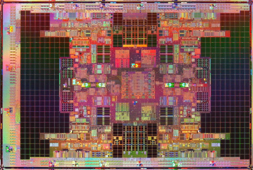
has die photograph!
14nm... interesting.
straight scaling would suggest 16nm. Previously Intel talked about 15nm as their next process. It could be just a naming thing, but maybe Intel is aiming for >2 area scaling from 22nm.
The Original 'IPAD'?
sad sad sad...
It had a touch-screen display, was powered by an ARM processor, featured a built-in MP3 player and it let you surf the Internet on your couch. Sound familiar? Think again. This was the Intel PAD or, as it was known internally at the time, the IPAD. It was officially branded the Intel Web Tablet, but it never made it to market.
So the course changed as Grove weighed in. Now, the tablet would be an Intel- branded product. At the time, Intel was also designing and building a host of other branded products, including digital cameras, wireless keyboards and mice, and a line of connected toys with Mattel. Grove saw this as a natural extension of the business that would help sell more PCs.
IBM 'fab club' switches high-k camps
http://www.eetimes.com/electronics-news/4212271/IBM--fab-club--switches-high-k-camps
Ivy Bridge (22nm microprocessor) is back from the fab and functioning well, according to Otellini.
To put that in context
- Penryn had its first public demo on January 27th, 2007.
- Westmere had its first public demo on February 10th, 2009.
Where is this chip???
Lincroft is ready, but the "Whitney Point" southbridge is not.
This will add SATA, HDMI and "legacy IO".
IMO this was Intel's biggest mistake, that Intel focused too much on "smart phones" with Moorestown.
http://www.mydigitallife.info/2010/06/02/intel-oak-trail-dual-core-atom-n455-and-n475-annoucement-at-computex/" rel="nofollow" target="_blank" >http://www.mydigitallife.info/2010/06/02/intel-oak-trail-dual-core-atom-n455-and-n475-annoucement-at-computex/
Intel on 15nm, Beyond CMOS Technologies
We have been smoothly scaling down planar CMOS until the 22nm generation, but there will be a major turning point in the 15 to 11nm generations. We will have two options, fin FET (field effect transistor) or fully-depleted SOI (silicon on insulator) transistor.
Intel will employ fin FETs because they have some advantages over fully-depleted SOI transistors.
GlobalFoundries "is closing the gap with Intel" on leading-edge technology introductions. "By going to a shared technology development model with IBM," he said, "we are closing the gap. We were a year behind Intel at the 45 nm node, and that difference will be cut significantly at the 32 nm generation. By 22 nm, there will be no difference. It will be in the noise level."
Re: Westmere-EX
Lower core count also helps with SER (silent error rate) characteristics.
Also Intel has to fight Amdahl's law at these high thread counts.
2.26 GHz base frequency was very low with Beckton, so let's say 2.53 GHz base for Westmere-EX is not very high and still in the "low voltage" region for 32nm.
Intel investor meeting 2010 in progress..
here are some slides:
http://intelstudios.edgesuite.net/im/home.htm
I'm looking at it right now, but some things I noticed:
Bill Holt:
- saved >400m$ for not using immersion lith at 45nm.
- saving >500m$ each generation for not doing SOI.
- yield curve at slide 16, 32nm is not a smooth as 45nm, but getting there.
Dadi Perlmutter:
- Sandy Bridge will have improved hyper-threading.
- "Cedar Trail" name for next netbook generation is confirmed.
- on-die vs. on-package MC is only a few nanoseconds.
- Nehalem has out-of-order execution, bigger cache, and advanced prefetching compard to Atom.
So the answer is no.
you list peak flops for ATI and Nvidia.
it seems SGEMM flops/s is about one third of peak for current GPUs.
http://www.heise.de/newsticker/meldung/SC09-Intel-demonstriert-Larrabee-mit-ueber-1-Teraflops-862305.html
software licesing cost will be interesting then.
i.e. will software vendors treat one Bulldozer module as just one physical core.
Westmere demoed.
some pictures from the event are on intels ftp...
ftp://download.intel.com/pressroom/kits/32nm/westmere/
i guess we´ll hear more on the web soon..
32nm IEDM presentation pdf
http://download.intel.com/technology/architecture-silicon/32nm/iedm_2008_32nm_foils.pdf
32nm PMOS almost as fast as 45nm NMOS.
Jan 10, 2006
You can kill a man, but you can't kill an idea.
- Hector Ruiz, 2008
Intel multicore briefing
lots of pdfs to download
http://www.intel.com/pressroom/archive/releases/20080317fact.htm?iid=pr1_releasepri_20080317fact
what's the relevance for AMD?
Is this your AMD/SUN/anti-intel fanboy clubhouse (called "Little Spaceship Crashed") ?
Live Intel webcast - Investor Meeting
http://intel_im.edgesuite.net/2008/index.htm
(retracted)
I thought wbmw wrote "Intel has no 65 nm chipsets this year" and quickly fired off a reply, before reading on ... doh
Shanghai sample running at 1.64 volt !
seems like an AMD-modified CPU-Z to hide MHZ, so I guess the voltage reading is correct.
look at the gallery:
http://www.computerbase.de/news/hardware/prozessoren/amd/2008/maerz/amd_45-nm-prozessor/
Re : So for 128GB of memory, it costs $25,485.00 to populate.
With this new MetaRAM, Colfax offers a 256 GB AMD quad-socket server for $45,000:
http://www.colfax-intl.com/jlrid/SpotLight_more_Acc.asp?L=120&S=42&B=1475
The ram is only PC2-4200 (533 Mhz), though.
well maybe I've overreacted ..
but "cheap" 256 gbyte systems could be nice for AMD.
yep ;)
well there will be a DDR3 version of MetaSDRAM for Nehalem.
Meanwhile, AMDs old platforms get a kick for RAM hungry HPC and virtualization workloads.
Fred Weber saves AMD's ass
MetaSDRAM MR08G2 chipset enables 2-rank 8GB DIMMs and is capable of
functioning at speeds up to 667MT/s. It consists of an AM150 Access Manager
and 5 FC540 Flow Controllers working as a group. The chipset is currently
in full production and is available at $200 each in 1,000 kit quantities.
http://www.foxbusiness.com/markets/industries/technology/article/metaram-develops-new-technology-quadruples-memory-capacity-servers_491760_12.html
-------------
Intel with FB-DIMM will not profit from this.
Caneland is toast.
Tukwila die shot
"dual integrated memory controllers"
http://www.hexus.net/content/item.php?item=11578
didn't you claim on SI that Conroe corrupted the Windows registry ?
What if a Barcelona server crashes while writing to the registry ?
April 2006 ... strange that Woodcrest only mas-paper-launched in June 2006 ..
mmoy,
actually, only quad core LGA775 parts are delayed to "Q1" due to the FSB marginality problem.
These parts will launch with new C1 / M1 steppings.
Core 2 Quad Q9300 is M1 stepping with 2 x 79 sqmm die size !
see page 15 here :
http://download.intel.com/design/processor/specupdt/31872704.pdf
OT btw, new Futurama movie on DVD is avaiable.
Mobile Penryn data sheet
ftp://download.intel.com/design/mobile/datashts/31891401.pdf
"When the core enters C6, it saves the processor state that is relevant to the processor
context in an on-die SRAM that resides on a separate power plane VCCP (I/O power
supply). This allows the main core VCC to be lowered to a very low-voltage VC6."
V_C6 = 0.35 - 0.7 Volt
Page 72 : TDP
0.3 Watt for Deep Power Down
-----------
specification update:
ftp://download.intel.com/design/mobile/SPECUPDT/31891501.pdf
page 9 : the T8000 series is offered as both C-0 stepping and M-0 Stepping (Penryn 3M) ! 200 MHz Dynamic Acceleration (Turbo Mode) boost.
Penryn 3M
die size ~79 mm2 and also more quadratic than penryn.
hopefully this will be out faster than allendale.
EDIT: at first I thought the 3MB photo was a photoshop job, but after looking at the left and right sides of the die closely, it could be real.
slide 38:
http://media.corporate-ir.net/media_files/irol/10/101302/UBSConfNov2007Bryant.pdf

