


Tuesday, December 27, 2022 11:48:33 AM
Patterned wafer inspection system
There are many types of patterned wafer inspection systems, including the electron beam inspection systems, the bright-field inspection systems, and the dark-field inspection systems. Each of these has its own features, but the basic detection principles are the same.
On a semiconductor wafer, electronic devices of the same pattern are made side by side. Random defects are often caused by particles such as dust and occur in random positions, as the name suggests. The possibility that they will occur repeatedly in a specific position is extremely low.
Patterned wafer inspection system can therefore detect defects by comparing the pattern images of adjacent chips (also called dies) and obtaining the difference.
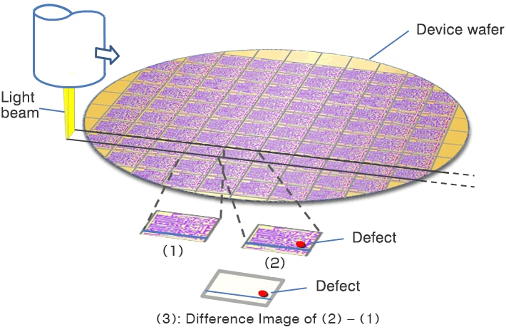
Fig.5-1 shows the principle for detecting defects on a patterned wafer.
The pattern on the wafer is captured along the die array by electron beam or light. Defects are detected by comparison between image (1) of the die to be inspected and image (2) of the adjacent die. If there are no defects, the result of the subtraction of Image 2 from Image 1 by digital processing will be zero and no defects are detected. In contrast, if there is a defect in the image of die (2), the defect will remain in the subtracted image (3) as shown in the figure. The defect is then detected and its position coordinates are registered.
Non-patterned wafer inspection system
The non-patterned wafer inspection system is used in the wafer shipping inspection by wafer manufacturers, the wafer incoming inspection by device manufacturers and the equipment condition check using dummy bare wafers to monitor the cleanliness of equipment. The equipment condition check is also performed by the equipment manufacturer at the shipping inspection and by the device manufacturer at the equipment incoming inspection.
To check the cleanliness of equipment, a bare wafer for cleanliness monitoring is loaded into the equipment and the stage inside the equipment is then moved to monitor the increase in particles.
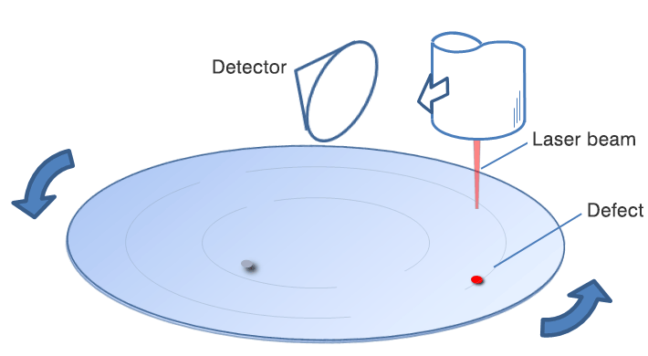
Fig.5-2 shows the principle for detecting defects on a non-patterned wafer.
Since there is no pattern, defects are detected directly without image comparison.
A laser beam is projected to the rotating wafer and is moved in the radial direction so that the laser beam is able to irradiate entire surface of the wafer.
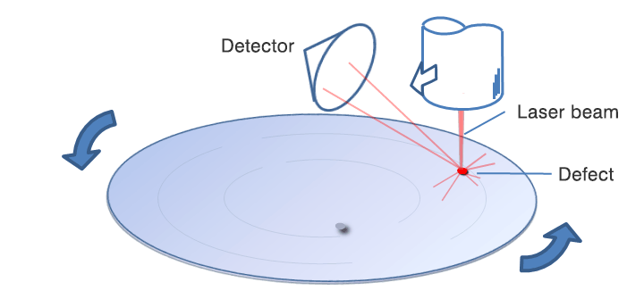
Fig.5-3. Principle of defect detection on a non-patterned wafer(2)
When a laser beam is projected onto a particle/defect of a rotating wafer, the light will be scattered and detected by a detector. Thus, the particle/defect is detected. From the wafer rotation angle and the radius position of the laser beam, the position coordinates of the particle/defect are calculated and registered. Defects on a mirror wafer also include crystal defects such as COP in addition to particles.
In general, the bright-field inspection system is intended for the detailed examination of pattern defects. On the other hand, the dark-field inspection system can detect at high speed and is intended for the defect inspection of a large number of wafers.
In the electron beam inspection system, electron beam is irradiated onto the surface of the wafer, and the emitted secondary electrons and backscattered electrons are detected.
Moreover, the electron beam inspection system detects the amount of the secondary electrons as an image contrast (voltage contrast) according to the conductivity of the device’s internal wiring. If the conductivity at the bottom of the contact hole of the high aspect ratio is detected, the SiO2 residue of ultra-thin thickness can be detected.
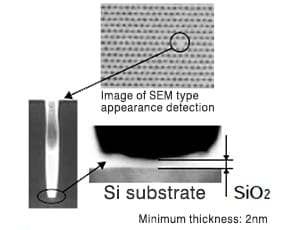
Fig.5-4. An example of detecting the residue at the bottom of a contact hole.
https://www.hitachi-hightech.com/global/en/knowledge/semiconductor/room/manufacturing/inspection.html

Recent LWLG News
- Form 3 - Initial statement of beneficial ownership of securities • Edgar (US Regulatory) • 08/13/2024 08:58:16 PM
- Form 8-K - Current report • Edgar (US Regulatory) • 08/12/2024 08:30:07 PM
- Lightwave Logic Provides Second Quarter 2024 Corporate Update • PR Newswire (US) • 08/12/2024 12:31:00 PM
- Form 10-Q - Quarterly report [Sections 13 or 15(d)] • Edgar (US Regulatory) • 08/09/2024 08:14:43 PM
- Form 424B5 - Prospectus [Rule 424(b)(5)] • Edgar (US Regulatory) • 08/09/2024 08:10:18 PM
- Form 424B5 - Prospectus [Rule 424(b)(5)] • Edgar (US Regulatory) • 08/09/2024 08:08:25 PM
- Form EFFECT - Notice of Effectiveness • Edgar (US Regulatory) • 08/06/2024 04:15:14 AM
- Form S-3/A - Registration statement under Securities Act of 1933: [Amend] • Edgar (US Regulatory) • 07/31/2024 09:05:40 PM
- Lightwave Logic Invited to Present at 2024 European Conference on Optical Communications • PR Newswire (US) • 07/30/2024 12:31:00 PM
- Form S-3 - Registration statement under Securities Act of 1933 • Edgar (US Regulatory) • 07/26/2024 09:07:10 PM
- Lightwave Logic Appoints Industry Veteran Yves LeMaitre to Board of Directors • PR Newswire (US) • 07/23/2024 12:31:00 PM
- Form 8-K - Current report • Edgar (US Regulatory) • 07/22/2024 08:47:34 PM
- Lightwave Logic Reaffirms Commercialization Timeline Presented at the 2024 Annual Shareholder Meeting • PR Newswire (US) • 06/03/2024 12:31:00 PM
- Form 8-K - Current report • Edgar (US Regulatory) • 05/24/2024 08:01:14 PM
- Lightwave Logic and Advanced Micro Foundry (AMF) Partner to Accelerate Development of Silicon Photonics Modulators Using Electro-Optic Polymers • PR Newswire (US) • 05/21/2024 12:31:00 PM
- Lightwave Logic Provides First Quarter 2024 Corporate Update • PR Newswire (US) • 05/13/2024 12:31:00 PM
- Form 10-Q - Quarterly report [Sections 13 or 15(d)] • Edgar (US Regulatory) • 05/10/2024 08:41:09 PM
- Lightwave Logic Demonstrates Thought Leadership with Critical Contributions to Global Integrated Photonics Industry Roadmap • PR Newswire (US) • 04/16/2024 12:31:00 PM
- Lightwave Logic Secures New Patent for Diamondoid Non-linear Optical Chromophore Patent to Improves Material Robustness • PR Newswire (US) • 04/01/2024 12:31:00 PM
- Lightwave Logic EO Polymer Achieves World-Class Performance of 400Gbps with Plasmonic Mach Zehnder Modulator • PR Newswire (US) • 03/28/2024 12:31:00 PM
- Lightwave Logic Demonstrates World-Class 200Gbps Heterogeneous Polymer/Silicon Photonic Modulator Results • PR Newswire (US) • 03/25/2024 12:31:00 PM
- Lightwave Logic to Host Annual Meeting of Shareholders on May 22, 2024 • PR Newswire (US) • 03/19/2024 12:31:00 PM
- Lightwave Logic to Participate in Upcoming Investor Conferences • PR Newswire (US) • 03/15/2024 12:31:00 PM
- Lightwave Logic Provides Fourth Quarter and Fiscal Year 2023 Corporate Update • PR Newswire (US) • 03/01/2024 01:31:00 PM
- Form 10-K - Annual report [Section 13 and 15(d), not S-K Item 405] • Edgar (US Regulatory) • 02/29/2024 10:09:53 PM
HealthLynked Corp. Announces Second Quarter and First Half 2024 Results: Continued Cost Reductions Set the Stage for Strategic Shift to App-Based Technology Services • HLYK • Aug 16, 2024 8:00 AM
PickleJar Announces Official Name Change and New Ticker Symbol • NREG • Aug 15, 2024 2:23 PM
VAYK's Q2 Profit Added to Accumulated Net Profit of Over $2.2 Million In 18 Months • VAYK • Aug 15, 2024 9:07 AM
Swifty Global Reports Strong Q2 Performance and Prepares for Major Exchange Uplisting • DRCR • Aug 15, 2024 9:04 AM
Mayback's Global Entertainment Signs Global Distribution Agreement with Children's Media Studio • AHRO • Aug 15, 2024 8:45 AM
POET Technologies Reports Second Quarter 2024 Financial Results • POET • Aug 15, 2024 8:04 AM

