 News
News  Market Data
  Discover
Support: 888-992-3836
Copyright © 2023 InvestorsHub Inc.


Register for free to join our community of investors and share your ideas. You will also get access to streaming quotes, interactive charts, trades, portfolio, live options flow and more tools.
GFOO is still GARBAGE...and ZERO Revenue.
GFOO one for 100 reverse split:
https://otce.finra.org/otce/dailyList?viewType=Symbol%2FName%20Changes
Check how thin this thing got on L2. Wonder why? :P ;)
Looking ready for some movements here. GFOO
$GFOO .0006 clearing and some ask pull. Super thin from here
$GFOO .0005x.0006 big bids showing @5 and lots of ask pull since last week. Action coming here soon
Do we know the potential acquirer yet?
GFOO The Potential Acquirer would obtain approximately 95% of our Common Stock and our then existing shareholders would retain approximately 5% of our Common Stock, resulting in significant dilution to our then existing shareholders
As of December 16, 2019, we had 9,124,901,879 shares of our Common Stock issued and outstanding.
95% of 9,124,901,879 = 8,668,656,785 ...
$GFOO .0003x.0004 super thin, possible move here imo
GENUFOOD ENERGY ENZYMES CORP. BECOMES PUBLIC REPORTING COMPANY IN U.S., ACHIEVES OTC PINK CURRENT INFORMATION STATUS
GlobeNewswire
8:00 AM ET
Genufood Energy Enzymes Corp. (OTC PINK:GFOO) (the "Company") announces that the Company has become a public reporting company under the Securities Exchange Act of 1934 and has achieved "Pink Current Information" status from OTC Markets.
The Company also reports that it has filed its Annual Report on Form 10-K for the fiscal year ended September 30, 2019.
"We are very pleased at the progress our current Board of Directors and management has made to bring the Company back into compliance with SEC and OTC Markets requirements, for the benefit of all our shareholders", said Kuang Ming (Jam es) Tsai, the Company's President and Chief Executive Officer. "Now that we are fully part of the SEC reporting system and OTC Markets shows that we have achieved "Pink Current Information" status, investors can more readily access information about our stock and analyze the Company's potential going forward", he continued.
"This is part of the ongoing commitment of our directors and management to improve our corporate transparency in anticipation of restarting our enzyme products business in Taiwan", observed Yi Ling (Betty) Chen, the Company's Treasurer and Secretary.
Safe Harbor Statement
This communication contains statements that may constitute "forward-looking statements" within the meaning of the Securities Act of 1933 and the Securities Exchange Act of 1934, as amended by the Private Securities Litigation Reform Act of 1995. Those statements include statements regarding the intent, belief or current expectations of Genufood Energy Enzymes Corp. and members of its management, as well as the assumptions on which such statements are based.
Prospective investors are cautioned that any such forward-looking statements are not guarantees of future performance and involve risks and uncertainties and that actua l results may differ materially from those contemplated by such forward-looking statements. Important factors currently known to management that could cause actual results to differ materially from those in forward-statements include, among other things, the having sufficient available capital to execute its plan of operations, regulatory compliance in Taiwan, market acceptance of the Company's enzyme products and the ability to compete successfully in a competitive environment.
CONTACT:
Betty Chen
Corporate Secretary
bettychen@geecenzymes.com
Lance Jon Kimmel
SEC Law Firm
www.seclawfirm.com
__GNW8366DE3E__IMG
Stick a Fork in GFOO.
The Potential Acquirer would obtain approximately 95% of our Common Stock and our then existing shareholders would retain approximately 5% of our Common Stock, resulting in significant dilution to our then existing shareholders
As of December 16, 2019, we had 9,124,901,879 shares of our Common Stock issued and outstanding.
95% of 9,124,901,879 = 8,668,656,785 ...
Bids at .0003 with this Dilution???????????????? SMHV
looking to maybe pick up some here...Vol way up all of a sudden
$GFOO Tier_Change: Pink No Information to Pink Limited
OTCM Link
https://www.otcmarkets.com/stock/GFOO/disclosure
Just skimmed over the latest 12g filing and they mention a possible R/S early next year subsequent to the company being aquired by another biopharmaceutical company. They also mention this: "the Potential Acquirer would obtain approximately 95% of our Common Stock and our then existing shareholders would retain approximately 5% of our Common Stock, resulting in significant dilution to our then existing shareholders"...
Talks of r/s in filing, cancelled my buy order.
got volume today but doesn't sustain it's pop we will see soon enough
YOU PUMP A FRAUD !!
People can easily verify that too.
You and your pumping pals from down under got exactly what you deserved.
NOTHING !!!!!
HAHAHAHAHAHAHAHA
I see you lost a SMME believer ( Pottsville) and a few others have wised up.
HOPE YA LOST A BUNDLE !!!!
Always lol at you !!!
DO YOUR OWN DD !!!
Or people could check themselves,
And then they can verify what I stated can be confirmed on the Nevada Secretary of State website.
My posts have always been concise, factual and rational too.
DON’T BELIEVE ANYTHING OPTIMISTICBUTPATIENT POSTS !!
That poster has been PUMPING that FRAUD called SMME for years.
I was booted off that board for spreading the truth on that scam. That was SMME and the pumpers only accomplishment. Lol
I do take take great comfort knowing that OBP and some of the other PUMPERS
Have lost a bundle of money.
Hey OBP. Where did all your pumping pals go ?
ALWAYS LMAO at you
ALWAYS DO YOUR OWN DD !!!
Reason tobinhood doesnt allow otc scams on teir platform i think all online brokets should follow
Ohhh ok i guess well wait till next week than
Re the Mergers button on the SOS site.
The mergers button for Genufood on the Nevada Secretary of State website lists a pending merger with Smartmetric, however if the same search is done for Smartmetric it states "No records to view."
Given this fact, as well as the Smartmetric CEO being unaware of any merger, it appears that there is no merger.
OBP.
SMME & GENUFOOD ARTICLES OF MERGER.
According to the Nevada Secretary of State website documents were filed on 14/8/2019 with reference number 20190096584 titled "Articles of Merger" for SMME.
On the same date Genufood also had documents filed with reference number 20190096584 titled "Articles of Merger".
The Nevada SOS site does not enable links to be posted to their pages but clicking on their link and entering Smartmetric or Genufood, also a Nevada company, will take you to the page which lists their Company details. Going to the filings link at the bottom of the page will take you to a list of all their respective filings.
At the present time the Nevada SOS site is having issues with displaying their documents so they cannot be viewed but this will hopefully be corrected next week.
I am a long term investor in Smartmetric and was taken aback by the sudden announcement on IHub and tracked down the Nevada SOS details and have queried the CEO about them.
At 23:55 on the 18th (Australian Eastern Time) she replied back to me with as follows;
"I am confirming that SMME is not merging with ANY company. This is an obvious attempted fraud.
Could be a criminal attempting to sell stock at a higher price in the supposed merger entity"
I have also spoken to the Company secretary and he is also unaware of any merger.
Given the fact that there are no similarities between Smartmetric and Genufood it seems highly unlikely that there would be any reason for a merger now or at any time in the future.
OBP.
How come that can be a fraud?
someone told me it was a fraud filling by someone out of the company to sell shares.... I tried contacting https://www.smartmetric.com/ but haven't got a reply.
I dont see the need for them to merge with this as it was pointed out to me... smme is otcqb. Im trying to do more dd.
Looking at the merging company, their share structure and capital value, and doing some math with GFOO structure and value, this is worth at least .0016+ without manipulation. And that is with SMME pps being low balled right now at lows, they average double that past few years. Not saying this is penny bound but there is at least a 400%+ jump from this level.
This is going to be interesting ??. $$
Nevada SOS site. Search genufood and look at filings, down at the bottom right there is a merger button, and takes you to the company merging with.
Where did u find that at?
Merging with "Smartmetric, Inc." according to the filings. They have a website https://www.smartmetric.com/about
Seems like a pretty decent operation. Currently trading .03 under SMME, this could get interesting.
.0006 is resis for now two times it has tested that past day and today but hasn't broken it. We will see if volume keeps up next week.
They accumulating and shaking us buyers at 4,5,6s before they run this but it's coming soon. They wouldn't be this aggressive last few days and today if it wasnt coming sooner then later.. JMO watching this ticker since Oct 2017.
whacky just about you think it's gonna break out with not much shares on ask get's dipped to .0003 again
Nice looks like shares being sold into the market. Once they are done it will blast off!!!
It can and will move very fast
Let us see
Exactly looks like shares being sold into this volume. Then news and blast off!!!
Something interesting happening here
I have been in it for years and never seen so much volume and movement
We will see
Been watching this since Oct 2017. Filings are way over due. Gonna assume recent volume are insiders loading up and trying shake the buyers at .0004, .0005 and .0006S before news hits.
once that support at .0004 got pulled you know it was gonna dip back
What a piece of $hit stock. Thought some followup on day 2 to continue hype but died in a day.
SCAM
jmo
0 volume. LOL no buyers one day P&D $hit show
jmo
Let's see volume today any upside or more like pump n dump. Chinese scams are hard to believe
jmo
|
Followers
|
80
|
Posters
|
|
|
Posts (Today)
|
0
|
Posts (Total)
|
5302
|
|
Created
|
09/10/12
|
Type
|
Free
|
| Moderators | |||


m.sg/wpcontent/uploads/2014/GESPLOrganizationCHART2014.pdf
Recently moved their office to
Figueroa at Wilshire
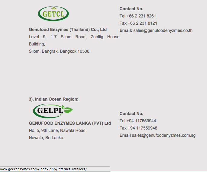
Sole Distributors
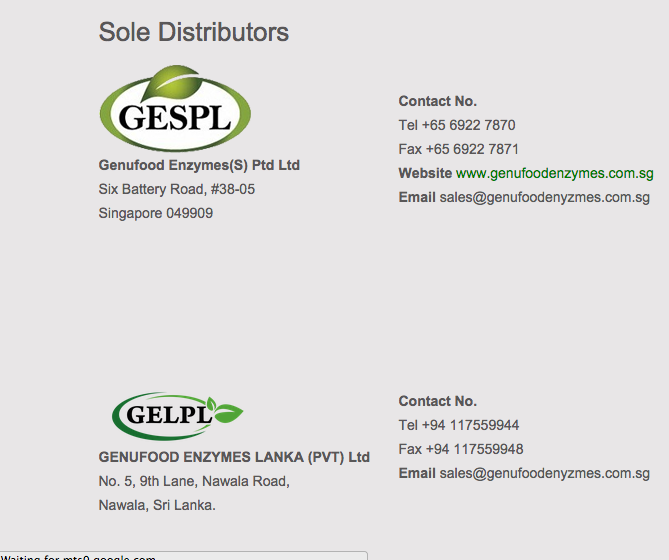
Internet Retailers

Website: http://www.geecenzymes.com
Phone: (713) 353-8834
Email: oliver@geecenzymes.com
Product Purchase Website and major subsidiary out of Singapore:
http://www.genufoodenzymes.com.sg/
Which Has Been Recently Updated as of October 2014 and is Still being Updated.

http://www.afscapitalmarkets.com/amcm/pdf/ProCellax-SNU.pdf
http://naturesfarm.com/files/1401437520289.pdf
On September 25, 2014, Genufood Energy Enzymes Corp. (the “Company”) completed a share exchange (the “Share Exchange”) with 100% of the issued and outstanding shares of Natfresh Beverages Corp. (“Natfresh”). The Share Exchange was approved by a majority vote of the shareholders of both the Company and Natfresh, by written consent. Pursuant to the Share Exchange, the Company issued shares of common stock to the shareholders of Natfresh on a 1 for 1 basis. The Company has issued a total of 1,156,460,641 shares of common stock to the shareholders of Natfresh. After the Share Exchange, Natfresh has become a wholly-owned subsidiary of the Company and the Company has acquired all of its assets and liabilities. As of Natfresh’s audited financial statements for the year ended August 31, 2013, Natfresh had total assets of $989,857, including cash of $785,312, total liabilities of $190,445 and stockholders’ equity of $799,412.
http://www.natfreshbeverages.com
 United States of America
 Singapore
 Malaysia
 Thailand
 Hong Kong
 Taiwan
 Macau
Macau China
China Indonesia
 Sri lanka
GFOO Security Details
Share Structure
Market Value $3,648,090 a/o Oct 10, 2014
Shares Outstanding 429,186,859 a/o Jul 31, 2014
Float 35,406,417 a/o Aug 28, 2014
Authorized Shares 3,000,000,000 a/o Oct 10 2014
Par Value 0.001
Shareholders of Record 135 a/o Jul 31, 2014
_____________________________________________________________________________________________________________________________________________________________________________________________________________________________________________________________
IBOX UPDATED ON 09/26/2017 - PER ADMIN - NO USER CAN DELETE ANOTHER USERS
INFORMATION AND IT SHOULD BE BELOW ANOTHER USERS CONTENT
_____________________________________________________________________________________________________________________________________________________________________________________________________________________________________________________________
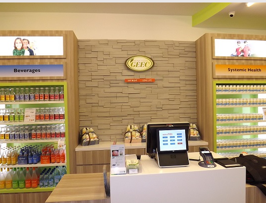
1st Thing I DID, TESTED COMPANY WEBSITE - THE COMPANY IS STILL TAKING ORDERS, WHICH I DID NOT EXPECT AT ALL!!!
![]()

Welcome to GESPL!

Genufood Enzymes (S) Pte Ltd
Level 27, Prudential Tower, 30 Cecil Street,
Singapore 049712
Tel : +65 8111 1822
Fax : +65 6631 2880

Register with us for future convenience:
Register with us for future convenience:
Please log in below:
Billing Information
 Loading next step... Loading next step... Loading next step...
* Required Fields
Continue Loading next step...| Product Name | Price | Qty | Subtotal |
|---|---|---|---|
| Subtotal | S$900.00 | ||
| Shipping & Handling (Free Delivery Singapore - Free Delivery) | S$0.00 | ||
| Grand Total | S$900.00 | ||
ProCellax DG1 | S$90.00 | 10 | S$900.00 |
Forgot an Item? Edit Your Cart
Place Order Submitting order information...THE NEXT THING I DID WAS - CHECKED THERE FACEBOOK PAGE


Mr. Ching Ming Hsu is President & Investor Relations Officer at New Palace International Co. Ltd. He is on the Board of Directors at Honmyue Enterprise Co., Ltd.
He received his graduate degree from Tunghai University.
THIS COMPANY RUN BY OUR NEW CEO IS PROFITABLE AND PAYS A 5% DIVIDEND YIELD!!!
SIGNIFICANT EXPERTIES AND INTELLECTUAL PROPERTY.
PATENTS OWNED BY CEO ARE QUITE INTRIGUING!
Patents by Inventor Ching-Ming Hsu
Ching-Ming Hsu has filed for patents to protect the following inventions. This listing includes patent applications that are pending as well as patents that have already been granted by the United States Patent and Trademark Office (USPTO).
OFFLINE-OPERABLE WIRELESS NETWORK SYSTEM AND METHOD FOR OPERATING THE SAME
Publication number: 20170265123
Abstract: The present invention relates to an offline-operable wireless network system and. the method for operating the same. When a wireless base station is not connected to the evolved packet core (EPC) server, the wireless base station will emulate the EPC server. Thereby, the electronic device connected with the wireless base station can be connected to the emulated EPC server, so that the wireless network functions still can be applied in the offline state and a wireless local area network can be further built.
Type: Application
Filed: May 13, 2016
Publication date: September 14, 2017
Inventors: CHING-SUNG HSU, SHIH-CHIANG YANG, PAO-CHING TSENG, FU-MING YEH
Semiconductor light emitting device and method of fabricating the same
Patent number: 9735312
Abstract: A method of manufacturing a semiconductor light-emitting device, comprises the steps of providing a first substrate; providing multiple epitaxial units on the first substrate, wherein the plurality of epitaxial units comprises: multiple first epitaxial units, wherein each of the first epitaxial units has a first geometric shape and a first area; and multiple second epitaxial units, wherein each of the second epitaxial units has a second geometric shape and a second area; providing a second substrate with a surface; transferring the multiple second epitaxial units to the surface of the second substrate; and dividing the first substrate to form multiple first semiconductor light-emitting devices, wherein each of the first semiconductor light-emitting devices has the first epitaxial unit; wherein the first geometric shape is different from the second geometric shape, or the first area is different from the second area.
Type: Grant
Filed: July 3, 2013
Date of Patent: August 15, 2017
Assignee: EPISTAR CORPORATION
Inventors: Hsin-Chih Chiu, Chih-Chiang Lu, Chun-Yu Lin, Ching-Huai Ni, Yi-Ming Chen, Tzu-Chieh Hsu, Ching-Pei Lin
Apparatus and method for reducing optical cross-talk in image sensors
Patent number: 9711562
Abstract: A method includes forming a plurality of pixels formed on a front surface of a semiconductor substrate, forming an array of color filters over the plurality of pixels, each color filter being adapted for allowing a wavelength of light radiation to reach at least one of the plurality of pixels, forming a plurality of micro-lenses over the array of color filters, and forming a second layer between the pixels and the color filters. The second layer further includes a structure adapted for blocking light radiation that is traveling towards a region between adjacent micro-lens, further wherein the plurality of micro-lenses are in contact with the array of color filters, and wherein the structure and the transparent material are coplanar at respective top surfaces thereof, and further wherein the structure directly contacts a bottom surface of at least one of the color filters.
Type: Grant
Filed: October 17, 2016
Date of Patent: July 18, 2017
Assignee: Taiwan Semiconductor Manufacturing Company, Ltd.
Inventors: Chin-Min Lin, Ching-Chun Wang, Dun-Nian Yaung, Chun-Ming Su, Tzu-Hsuan Hsu
COATING APPARATUS FOR CONTINUOUSLY FORMING A FILM THROUGH CHEMICAL VAPOR DEPOSITION
Publication number: 20170191162
Abstract: A coating apparatus for continuously forming a film through chemical vapor deposition (CVD) includes a conveyor unit for conveying a substrate along a moving path, a deposition unit and a film formation-prohibiting unit. The deposition unit is disposed on the moving path and includes a deposition chamber adapted for receiving the substrate and forming a film on the substrate through CVD. The film formation-prohibiting unit includes a heating mechanism that is disposed in the deposition chamber for maintaining the conveyor unit at a film formation-prohibiting temperature.
Type: Application
Filed: December 30, 2015
Publication date: July 6, 2017
Inventors: TING-PIN CHO, WEN-CHENG KUO, KUNG-MING HSU, CHING-FU YANG, JYH-NAN SHIEH
Semiconductor structure and method for manufacturing the same
Patent number: 9691704
Abstract: A semiconductor structure comprises a first wire level, a second wire level and a via level. The first wire level comprises a first conductive feature. The second wire level is disposed on the first wire level. The second wire level comprises a second conductive feature and a third conductive feature. The via level is disposed between the first wire level and the second wire level. The via level comprises a via connecting the first conductive feature and the second conductive feature. There is a first air gap between the first conductive feature and the second conductive feature. There is a second air gap between the second conductive feature and the third conductive feature. The first air gap and the second air gap are linked.
Type: Grant
Filed: June 7, 2016
Date of Patent: June 27, 2017
Assignee: UNITED MICROELECTRONICS CORP.
Inventors: Kuo-Chih Lai, Chia-Chang Hsu, Nien-Ting Ho, Ching-Yun Chang, Yen-Chen Chen, Shih-Min Chou, Yun-Tzu Chang, Yang-Ju Lu, Wei-Ming Hsiao, Wei-Ning Chen
Polishing pad with offset concentric grooving pattern and method for polishing a substrate therewith
Patent number: 9687956
Abstract: The invention provides a polishing pad and a method of using the polishing pad for chemically-mechanically polishing a substrate. The polishing pad comprises a plurality of grooves composed of at least a first plurality of concentric grooves having a first center of concentricity, and a second plurality of concentric grooves having a second center of concentricity. The first center of concentricity is not coincident with the second center of concentricity, the axis of rotation of the polishing pad is not coincident with at least one of the first center of concentricity and the second center of concentricity, the plurality of grooves does not consist of a continuous spiral groove, and the polishing surface does not comprise a mosaic groove pattern.
Type: Grant
Filed: November 5, 2013
Date of Patent: June 27, 2017
Assignee: Cabot Microelectronics Corporation
Inventors: Ching-Ming Tsai, Shi-Wei Cheng, Kun-Shu Yang, Jia-Cheng Hsu, Sheng-Huan Liu, Feng-Chih Hsu, Craig Kokjohn
METHOD OF FORMING DEEP TRENCH ISOLATION IN RADIATION SENSING SUBSTRATE AND IMAGE SENSOR DEVICE
Publication number: 20170154917
Abstract: A method of forming a deep trench isolation in a radiation sensing substrate includes: forming a trench in the radiation sensing substrate; forming a corrosion resistive layer in the trench, in which the corrosion resistive layer includes titanium carbon nitride having a chemical formula of TiCxN(2?x), and x is in a range of 0.1 to 0.9; and filling a reflective material in the trench and over the corrosion resistive layer.
Type: Application
Filed: February 19, 2016
Publication date: June 1, 2017
Inventors: Chi-Ming LU, Chih-Hui HUANG, Jung-Chih TSAO, Yao-Hsiang LIANG, Chih-Chang HUANG, Ching-Ho HSU
MICROFLUIDIC DUAL-WELL DEVICE FOR HIGHTHROUGHPUT SINGLE-CELL CAPTURE AND CULTURE
Publication number: 20170145363
Abstract: A microfluidic dual-well device is disclosed. The device comprises: (a) a first substrate having a first end, a second end, and a culture microwell forming portion; (b) a plurality of culture microwells; (c) a second substrate having a first end, a second end, and a capture microwell forming portion, the two ends of the second substrate being respectively bounded to the two ends of the first substrate; (d) a plurality of capture microwells; (e) a microfluidic channel; (f) a microfluidic inlet port; and (g) a microfluidic outlet port; wherein the microfluidic channel is in fluidic connections with the culture microwells, the capture microwells, and the inlet and outlet ports. Methods of capturing and transferring a single cell or a single cell colony for culture, and method of transferring a target cell from a polydimethylsiloxane (PDMS) structure of culture microwells to a culture plate for culture are also disclosed.
Type: Application
Filed: May 19, 2016
Publication date: May 25, 2017
Inventors: Chia-Hsien HSU, Ching-Hui LIN, Duane S. JUANG, Hao-Chen CHANG, Ing-Ming CHIU
SEMICONDUCTOR DEVICE AND METHOD FOR FABRICATING THE SAME
Publication number: 20170148891
Abstract: A method for fabricating semiconductor device is disclosed. The method includes the steps of: providing a substrate having a first region, a second region, a third region, and a fourth region; forming a tuning layer on the second region; forming a first work function metal layer on the first region and the tuning layer of the second region; forming a second work function metal layer on the first region, the second region, and the fourth region; and forming a top barrier metal (TBM) layer on the first region, the second region, the third region, and the fourth region.
Type: Application
Filed: November 24, 2015
Publication date: May 25, 2017
Inventors: Kuo-Chih Lai, Yun-Tzu Chang, Wei-Ming Hsiao, Nien-Ting Ho, Shih-Min Chou, Yang-Ju Lu, Ching-Yun Chang, Yen-Chen Chen, Kuan-Chun Lin, Chi-Mao Hsu
Semiconductor process of forming metal gates with different threshold voltages and semiconductor structure thereof
Patent number: 9659937
Abstract: A semiconductor process of forming metal gates with different threshold voltages includes the following steps. A substrate having a first area and a second area is provided. A dielectric layer and a first work function layer are sequentially formed on the substrate of the first area and the second area. A second work function layer is directly formed on the first work function layer of the first area. A third work function layer is directly formed on the first work function layer of the second area, where the third work function layer is different from the second work function layer. The present invention also provides a semiconductor structure formed by said semiconductor process.
Type: Grant
Filed: April 9, 2015
Date of Patent: May 23, 2017
Assignee: UNITED MICROELECTRONICS CORP.
Inventors: Ching-Yun Chang, Chi-Mao Hsu, Wei-Ming Hsiao, Nien-Ting Ho, Kuo-Chih Lai
3D IMAGE APPARATUS AND METHOD FOR DISPLAYING IMAGES
Publication number: 20140192033
Abstract: A three-dimensional (3D) image apparatus is provided. The 3D image apparatus includes a display unit, a front camera, and a processor. The front camera captures an image of the eyes of the user. The processor is coupled to the display unit and the front camera. The processor determines the position of the eyes of the user based on the image of the eyes of the user, and determines whether to display a 3D image or a two-dimensional (2D) image on the display based on the position of the eyes of the user.
Type: Application
Filed: January 7, 2013
Publication date: July 10, 2014
Applicant: HTC CORPORATION
Inventors: Ching-Ming Hsu, Yi-Yuan Hsieh, Po-Chang Ho
Fabrication method and structure of an ITO anode containing nickel points for an OLED to selectively light
Patent number: 7615285
Abstract: A fabrication method of an indium tin oxide (ITO) anode containing point nickel for an organic light emitting diode (OLED) to selectively light includes various processes of preparing an ITO substrate with an anode having plural point grooves, of forming a nickel film on the anode, and of grinding the nickel film to leave the point grooves fitted with nickel. Therefore, the nickel spots of the ITO anode are lit up earlier than the pure ITO anode when the OLED is turn on. Because the nickel spots have a lower resistance, current can aggregate in these spots collectively, reducing demerit of cross-talk happening often in a conventional passive OLED panel circuit. The structure of the OLED includes an ITO substrate with an anode provided point grooves deposited with nickel, a hole transport layer on the anode, and an electron transport layer on the hole transport layer.
Type: Grant
Filed: June 21, 2006
Date of Patent: November 10, 2009
Assignee: Southern Taiwan University
Inventors: Ching-Ming Hsu, Wen-Tuan Wu, Chung-Lin Tsai
Fabrication method and structure of an ITO anode containing nickel points for an OLED to selectively light
Publication number: 20070298222
Abstract: A fabrication method of an indium tin oxide (ITO) anode containing point nickel for an organic light emitting diode (OLED) to selectively light includes various processes of preparing an ITO substrate with an anode having plural point grooves, of forming a nickel film on the anode, and of grinding the nickel film to leave the point grooves fitted with nickel. Therefore, the nickel spots of the ITO anode are lit up earlier than the pure ITO anode when the OLED is turn on. Because the nickel spots have a lower resistance, current can aggregate in these spots collectively, reducing demerit of cross-talk happening often in a conventional passive OLED panel circuit. The structure of the OLED includes an ITO substrate with an anode provided point grooves deposited with nickel, a hole transport layer on the anode, and an electron transport layer on the hole transport layer.
Type: Application
Filed: June 21, 2006
Publication date: December 27, 2007
Applicant: Ching-Ming HSU
Inventors: Ching-Ming Hsu, Wen-Tuan Wu, Chung-Lin Tsai
Fabrication method and structure of an ITO anode containing nickel for improving injection efficiency of an OLED
Publication number: 20070298283
Abstract: A fabrication method of an indium tin oxide (ITO) anode containing nickel for improving injection efficiency of an organic light emitting diode (OLED) includes various processes of preparing an ITO substrate with an anode, of preparing a target source of ITO containing nickel, and of mingling nickel on the anode of the ITO substrate by sputtering. The structure of the ITO anode containing nickel for an OLED includes a substrate with an anode mingled with nickel, a hole transport layer and an electron transport layer. Such an ITO anode is to have a higher work function that can lessen a great potential barrier between the ITO anode and a hole transport layer. So the threshold voltage and the turn-on voltage of OLED can be reduced to advance hole injection efficiency.
Type: Application
Filed: June 21, 2006
Publication date: December 27, 2007
Applicant: Ching-Ming HSU
Inventors: Ching-Ming Hsu, Wen-Tuan Wu, Hsin-Hui Lee
https://patents.justia.com/inventor/ching-ming-hsu
KEY TECHNOLOGY OWNED BY GFOO'S NEW CEO
THIN FILM SOLAR TECHNOLOGY
Morphology, composition and electrical properties of SnO2:Cl thin films grown by atomic layer deposition
Abstract
Chlorine doped SnO2 thin films were prepared using atomic layer deposition at temperatures between 300 and 450°C using SnCl4 and H2O as the reactants. Composition, structure, surface morphology, and electrical properties of the as-deposited films were examined. Results showed that the as-deposited SnO2 films all exhibited rutile structure with [O]/[Sn] ratios between 1.35 and 1.40. The electrical conductivity was found independent on [O]/[Sn] ratio but dependent on chlorine doping concentration, grain size, and surface morphology. The 300°C-deposited film performed a higher electrical conductivity of 315S/cm due to its higher chlorine doping level, larger grain size, and smoother film surface. The existence of Sn2+ oxidation state was demonstrated to minimize the effects of chlorine on raising the electrical conductivity of films.
Morphology, composition and electrical properties of SnO2:Cl thin films grown by atomic layer deposition.
Available from: https://www.researchgate.net/publication/283666514_Morphology_composition_and_electrical_properties_of_SnO2Cl_thin_films_grown_by_atomic_layer_deposition [accessed Sep 24, 2017]
https://www.researchgate.net/publication/283666514_Morphology_composition_and_electrical_properties_of_SnO2Cl_thin_films_grown_by_atomic_layer_deposition
SOLAR POWER TECHNOLOGY
High voltage and efficient bilayer heterojunction solar cells based on an organic-inorganic hybrid perovskite absorber with a low-cost flexible substrate
https://www.researchgate.net/publication/260271782_High_voltage_and_efficient_bilayer_heterojunction_solar_cells_based_on_an_organic-inorganic_hybrid_perovskite_absorber_with_a_low-cost_flexible_substrate
Impressive Stuff, created by the NEW CEO
STARTING TO THINK THIS IS A REVERSE MERGER PLAY, BASED ON THE INTELLECTUAL PROPERTY HE OWNS. HE IS ALSO RUNNING A $1.5 BILLION COMPANY SO IT COULD BE A SPIN OFF.
TRYING TO UNDERSTAND WHAT THE PLAN IS.
Light extraction enhancement of organic lightemitting diodes using aluminum zinc oxide embedded anodes Ching-Ming Hsu,* Bo-Ting Lin, Yin-Xing Zeng, Wei-Ming Lin, and Wen-Tuan Wu Department of Electro-Optical Engineering, Southern Taiwan University of Science and Technology, 1, Nan-Tai St., Yung-Kang District, Tainan City 710, Taiwan *tedhsu@mail.stust.edu.tw Abstract: Aluminum zinc oxide (AZO) has been embedded onto indium tin oxide (ITO) anode to enhance the light extraction from an organic lightemitting diode (OLED). The embedded AZO provides deflection and scattering interfaces on the newly generated AZO/organics and AZO/ITO interfaces rather than the conventional ITO/organic interface. The current efficiency of AZO embedded OLEDs was enhanced by up to 64%, attributed to the improved light extraction by additionally created reflection and scattering of emitted light on the AZO/ITO interfaces which was roughed in AZO embedding process. The current efficiency was found to increase with the increasing AZO embedded area ratio, but limited by the accompanying increases in haze and electrical resistance of the AZO embedded ITO film. ©2014 Optical Society of America OCIS codes: (290.5880) Scattering, rough surfaces; (230.3670) Light-emitting diodes; (230.4000) Microstructure fabrication; (310.6860) Thin films, optical properties.
https://www.osapublishing.org/captcha/?guid=1EBA91AE-BCE4-B8CC-1102-1CAC2D0A0E1B
ONE OF THE PATENTS OWNED BY THE CEO
Light Extraction Enhancement of Organic Light-Emitting Diodes Using Aluminum ..
Light Extraction Enhancement of Organic Light-Emitting Diodes Using Aluminum Zinc Oxide Embedded Anodes
CM Hsu et al. Opt Express 22 Suppl 7, A1695-A1700. 2014 Dec 15. more
Abstract
Aluminum zinc oxide (AZO) has been embedded onto indium tin oxide (ITO) anode to enhance the light extraction from an organic light-emitting diode (OLED). The embedded AZO provides deflection and scattering interfaces on the newly generated AZO/organics and AZO/ITO interfaces rather than the conventional ITO/organic interface. The current efficiency of AZO embedded OLEDs was enhanced by up to 64%, attributed to the improved light extraction by additionally created reflection and scattering of emitted light on the AZO/ITO interfaces which was roughed in AZO embedding process. The current efficiency was found to increase with the increasing AZO embedded area ratio, but limited by the accompanying increases in haze and electrical resistance of the AZO embedded ITO film.
PubMed: 25607483 DOI: 10.1364/OE.22.0A1695
https://www.ncbi.nlm.nih.gov/labs/articles/25607483/
http://mobile.reuters.com/finance/stocks/overview/1474.TW
http://quotes.wsj.com/TW/XTAI/1474/company-people/executive-profile/88924476
Date of Report (Date of earliest event reported): August 4, 2017
GENUFOOD ENERGY ENZYMES CORP.
(Exact name of registrant as specified in charter)
GFOO Security Details
Share Structure: The Freely Tradeable Float IS 1,161,148,975 -
CONFIRMED WITH TRANSFER AGENT SEPTEMBER 2017
THE TRANSFER AGENT STATED THE FOLLOWING:
THE PUBLIC FLOAT IS MUCH LOWER THAN THE CURRENT SHARES OUTSTANDING.
80% OF THE SHARES OUTSTANDING ARE HELD BY INSIDERS AND ARE "COMPLETELY RESTRICTED" AND CAN NOT BE SOLD INTO THE OPEN MARKET.
Quote:
Dean Law Corp. serves diverse clients on unique and sophisticated corporate and securities matters, initial public offerings, listing applications, reverse mergers, PIPEs, trademarks, corporate finance and M+As.
Our clients include well-established publicly and privately held corporations, emerging and development stage companies, entrepreneurial start up enterprises, private enterprise funds and other business entities across a broad range of industries.
Dean Law Corp.'s entrepreneurial spirit and competitive strength lies in its ability to blend its understanding of capital markets with its grasp of complex legal issues. Dean Law Corp.'s role as a valued business partner to numerous emerging growth clients, has allowed us to master the art of business and the science of law.

| ||||||||||||||||||||||||||||||||||||||||||||||||||||||||||||||||||||||||||
| |||||||||||||||||||||||||||||||||||||||||||||||||||||||||||||||||||||||||||||||||||||||||||||||||||||||||||||||||||||||||||
|
| Volume | |
| Day Range: | |
| Bid Price | |
| Ask Price | |
| Last Trade Time: |


 Click here to add optional extras ...
 Optional Items (select to add\remove optional fees to total above)
